购物车中还没有商品,赶紧选购吧!

 推荐用于新设计
特性
- GaN Drive Technology Fully Optimized for GaN FETs
- Output Voltage Up to 100V
- Wide VIN Range: 4V to 60V and Operates Down to 1V after Start-Up
- No Catch, Clamp, or Bootstrap Diodes Needed
- Internal Smart Bootstrap Switches Prevent Overcharging of High-Side Driver Supply
- Resistor-Adjustable Dead Times
- Split-Output Gate Drivers for Adjustable Turn On and Turn Off Driver Strengths
- Accurate Adjustable Driver Voltage and UVLO
- Low Operating IQ: 15μA
- Programmable Frequency (100kHz to 3MHz)
- Synchronizable Frequency (100kHz to 3MHz)
- Spread Spectrum Frequency Modulation
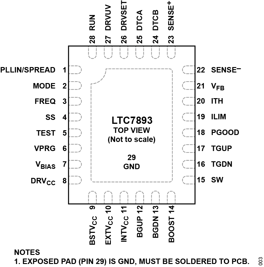
- 28-Lead (4mm × 5mm), Side Wettable, QFN Package
- AEC-Q100 Qualified for Automotive Applications
产品详情和应用
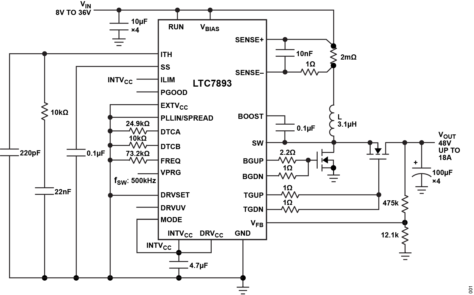
The LTC®7893 is a high performance, step-up, dc-to-dc switching regulator controller that drives all N-channel synchronous gallium nitride (GaN) field effect transistor (FET) power stages from output voltages up to 100V. The LTC7893 solves many of the challenges traditionally faced when using GaN FETs. The LTC7893 simplifies the application design while requiring no protection diodes and no other additional external components compared to a silicon metal-oxide semiconductor field effect transistor (MOSFET) solution.
The internal smart bootstrap switches prevent overcharging of the BOOST pin to the SW pin high-side driver supply during dead times, protecting the gate of the top GaN FET. The dead times of the LTC7893 can optionally be optimized with external resistors for margin or to tailor the application for higher efficiency and allowing for high frequency operation.
The gate drive voltage of the LTC7893 can be precisely adjusted from 4V to 5.5V to optimize performance, and to allow the use of different GaN FETs, or even logic level MOSFETs. When biased from the boost converter regulator output, the LTC7893 can operate from an input supply as low as 1V after start-up.
- Automotive and Industrial Power Systems
- Military Avionics and Medical Systems
- Telecommunications Power Systems