购物车中还没有商品,赶紧选购吧!

 推荐用于新设计
特性
- Ultra-low current consumption (typical)
- 32 μA: continuous conversion mode (gain = 128)
- 5 μA: duty cycling mode (ratio = 1/16)
- 0.5 μA: standby mode
- 0.1 μA: power-down mode
- Built-in features for system level power savings
- Current saving duty cycle ratio: 1/4 or 1/16
- Smart sequencer and per channel configuration minimizes host processor load
- Deep embedded FIFO minimizes host processor load (depth of 256 samples)
- Autonomous FIFO interrupt functionality, threshold detection
- Single supply as low as 1.71 V increasing battery length
- RMS noise: 25 nV rms at 1.17 SPS (gain = 128) = 48 nV/√Hz
- Up to 16 noise free bits (gain = 1)
- Output data rate: 1.17 SPS to 2.4 kSPS
- Operates from 1.71 V to 3.6 V single supply or ±1.8 V split supplies
- Band gap reference with 15 ppm/°C maximum drift
- PGA with rail-to-rail analog input
- Adaptable sensor interfacing functionality
- Matched programmable excitation currents for RTDs
- On-chip bias voltage generator for thermocouples
- Low-side power switch for bridge transducers
- Sensor open-wire detection
- Internal temperature sensor and oscillator
- Self and system calibration
- Flexible filter options
- Simultaneous 50 Hz/60 Hz rejection (on selected filter options)
- General-purpose outputs
- Diagnostic functionality
- Crosspoint multiplexed inputs
- 4 differential/8 pseudodifferential inputs
- 5 MHz SPI (3-wire or 4-wire)
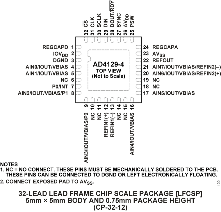
- Available in 35-ball, 2.7 mm × 3.56 mm WLCSP and 32-lead, 5 mm × 5 mm LFCSP
- Temperature range: −40°C to +105°C (WLCSP), −40°C to +125°C (LFCSP)
- AD4129-4 LFCSP pin compatible with AD712
产品详情和应用
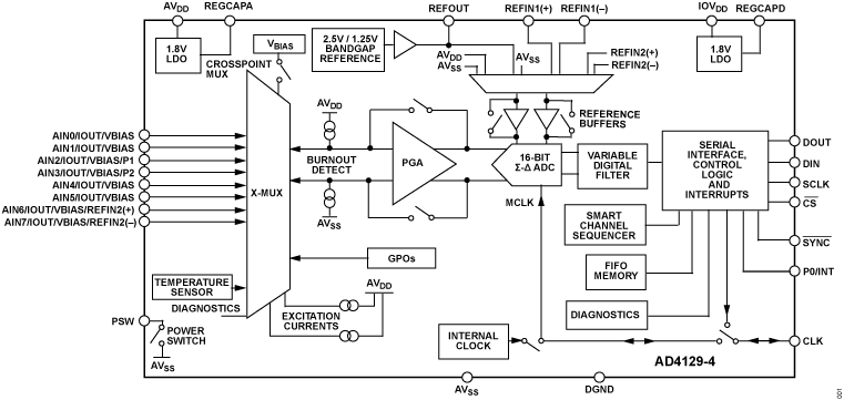
The AD4129-4 is an ultra-low power, high precision, and measurement solution for low bandwidth battery-operated applications. The fully integrated analog front end (AFE) includes a multiplexer for up to 8 single-ended or 4 differential inputs, programmable gain amplifier (PGA), 16-bit sigma-delta (Σ-Δ) analog-to-digital converter (ADC), on-chip reference and oscillator, selectable filter options, smart sequencer, sensor biasing and excitation options, diagnostics, and newly added features to improve the battery-operated lifetime (more than 5 years on a coin cell), that is, a first in, first out (FIFO) buffer and duty cycling.
The AD4129-4 allows users to measure low-frequency signals with a current consumption of 28.5 μA (gain = 1) and 32.5 μA (gain = 128) while continuously converting, and even lower average currents when using one of the duty cycling options. The AD4129-4 can be configured to have 4 differential inputs or 8 single-ended or pseudodifferential inputs, which connect to a crosspoint multiplexer, where any input pair can become a measurement channel input to the PGA and ADC.
The AD4129-4 is designed to allow the user to operate from a single analog supply voltage from 1.71 V to 3.6 V. In battery applications, operation as low as 1.71 V can extend the system lifetime as the AFE can continue its operation, even as the battery voltage dissipates. The digital supply can be separate and range from 1.65 V to 3.6 V.
Together with the reduced current consumption, the integration of an on-chip FIFO buffer can be used in tandem with the smart sequencer, to enable the AD4129-4 to become an autonomous measurement system, which allows the microcontroller to sleep for extended periods.
Intelligent interrupt functionality gives the user a greater confidence in both error detection and safety. The user can enable an interrupt signal to trigger when the samples in the FIFO reach a predefined va