购物车中还没有商品,赶紧选购吧!

 推荐用于新设计
特性
- Wideband integrated bidirectional bridge
- Raw directivity: 35.6 dB at 1 GHz, 16.7 dB at 18 GHz
- Low insertion loss: 1.1 dB at 1 GHz, 2.0 dB at 18 GHz
- Return loss: >12 dB typical
- SPI configurable LO interface
- Divide by 2; multiply by 1, 2, or 4
- Offset LO interface enables drive with fRF = fLO
- Single-ended or differential drive
- SYNC function—synchronization across multiple devices
- High dynamic range wideband IF signal path
- SPI-programmable IF bandwidth from 1 MHz to 100 MHz
- SPI-programmable IF gain, 6 dB step size
- Externally adjustable output common-mode level
- 5-bit SPI readable temperature sensor
- Low power shutdown mode
- 3 mm × 4 mm, 26-lead LGA
产品详情和应用
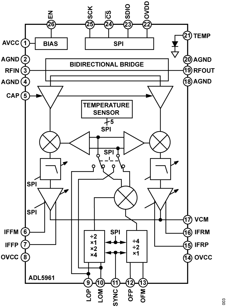
The ADL5961 is a wideband, small form factor, vector network analyzer (VNA) front end consisting of a resistive bidirectional bridge, downconversion mixers, programmable IF amplifiers and filters, and a highly flexible local oscillator (LO) interface. The bridge provides >14 dB of directivity up to 17 GHz. The primary transmission line from RFIN to RFOUT is wideband matched to 50 Ω with only 1.1 dB loss at 9 kHz near DC, increasing to 1.8 dB loss at 26.5 GHz.
The ADL5961 supports several different LO interface configurations that simplify the clocking design of a VNA solution as well as the interfacing of the device to an analog-to-digital converter (ADC). The frequency divider and multipliers in the LO interface enable measurement sweeps beyond the operating frequency range of the LO source, enabling operation over the full 26.5 GHz frequency range of the ADL5961 using a 6 GHz synthesizer. The IF frequency offset mixer, driven through the offset interface formed by the OFP and OFM pins, enables further simplification by allowing the swept RF and LO interfaces to share the same frequency source. The frequency of the IF output signals is then determined by the low-frequency source driving the OFP/OFM interface. When this interface is driven at the ADC sample frequency with the divide by 4 enabled, it automatically centers the IF output signal in the first Nyquist zone.
The IF filters with programmable bandwidth and IF amplifiers with individually programmable gain enable simultaneous dynamic range optimization of the IF output signals of the forward channel (IFFP, IFFM) and reverse channel (IFRP, IFRM). The IF amplifiers have an adjustable output common-mode level, sufficient drive capability, and wide output voltage swing to enable direct interfacing to a wide range of ADCs.
All configurations and functions in the ADL5961 are fully programmable through a 3-wire serial peripheral interface (SPI).