购物车中还没有商品,赶紧选购吧!

 推荐用于新设计
特性
- Wideband, 2 GHz to 18 GHz frequency range
- Quad input, single output
- True time delay core for wideband beam-squint free operation
- 0 ps to 508 ps range with 4 ps resolution
- 0 ps to 254 ps range with 2 ps resolution
- 31.5 dB gain adjustment range with 0.5 dB step size
- 4-bit pin-programmable device address setting
- On-chip sequencer
- Beam update via register, RAM, or FIFO
- Programmable amplifier bias
产品详情和应用
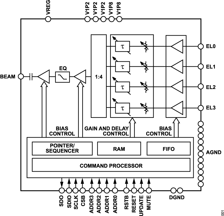
The ADAR4001 is a 2 GHz to 18 GHz quad-input, single-output beamformer IC (BFIC) that is optimized for phased array receive applications. A true, time delay based, core ensures beam-squint free wideband operation. The full-scale delay of the time delay unit (TDU) can be set to either 254 ps or 508 ps with a minimum step size of 2 ps and 4 ps, respectively. At 2 GHz, this results in a phase adjustment range of 365°, and at 18 GHz, the minimum phase step size is 13°.
Each path also has a 31.5 dB digital step attenuator (DSA) with a step size of 0.5 dB.
Control of all the on-chip registers is through a simple 3-wire or 4-wire serial port interface (SPI). Four address pins allow SPI control of up to 16 devices on the same serial lines.
The on-chip, random access memory (RAM) and first in, first out (FIFO) memory have storage for up to 64 and 16 beamstates, respectively. The on-chip sequencer can be used to select and advance the beamstate, which can be sourced from the RAM or FIFO.
The ADAR4001 is available in a 36-lead 6 mm × 6 mm LFCSP and is specified from −40°C to +85°C..
ADAR4001 is available in a 36-lead 6 mm × 6mm LFCSP package and is specified from −40°C to +85°C.
APPLICATIONS