购物车中还没有商品,赶紧选购吧!

 推荐用于新设计
特性
- 2 differential transmitters
- 2 differential receivers
- 2 differential observation receivers
- LO tunable range: 450 MHz to 7125 MHz
- RF range: 350 MHz to 7225 MHz1
- Maximum transmitter large-signal bandwidth: 200 MHz
- Maximum transmitter synthesis bandwidth: 450 MHz
- Maximum receiver signal bandwidth: 200 MHz
- Maximum observation receiver signal bandwidth: 450 MHz
- Fully integrated fractional-N RF synthesizer
- Fully integrated clock synthesizer
- Dual external LO inputs supporting operation up to 6 GHz
- JESD204B and JESD204C digital interface: up to 16.5 Gbps
- TDD and FDD operation
- Simplifying thermal and power consumption challenges
- 4.82 W power consumption for the TDD mode, enabled use case with 200 MHz iBW/OBW2
产品详情和应用
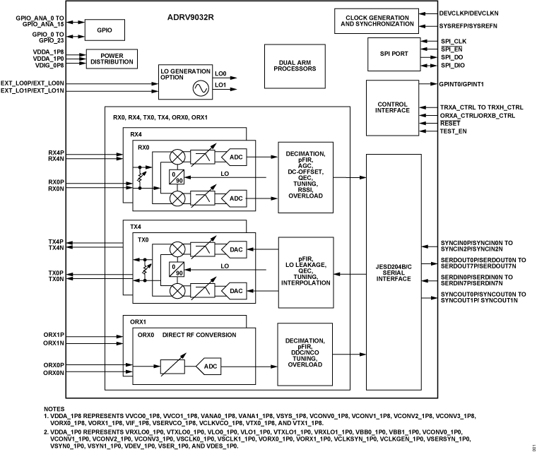
The ADRV9032R is a highly integrated, RF agile transceiver offering two transmitters, two observation receivers for monitoring transmitter channels, two receivers, integrated local oscillator (LO) and clock synthesizers, and digital-signal processing functions to provide a complete transceiver solution. The device provides the high radio performance and low-power consumption demanded by cellular infrastructure applications, software-defined radios, portable instruments, and military communications.
The receiver and transmitter signal paths use a zero-IF (ZIF) architecture that provides wide bandwidth with dynamic range suitable for non-contiguous multicarrier applications. The ZIF architecture has the benefits of low power and RF and bandwidth agility. The lack of aliases and out-of-band images eliminates anti-aliasing and image filters, reducing system size and cost, and making band independent solutions possible.
Please see the Data Sheet for the full description.
APPLICATIONS
- Software defined radios
- Portable instrumentation
- Military communications
- General-purpose radios
- Wireless infrastructure
- TDD and FDD applications