购物车中还没有商品,赶紧选购吧!

 预发布
预发布
特性
- Highly integrated transceiver
- 8 transmit (Tx), 8 receive (Rx), and 2 observation receivers (ORx)
- LO tuning range: 600 MHz to 7125 MHz
- RF range: 500 MHz to 7455 MHz1
- Zero-IF architecture reduces system size, weight, and power (SWaP)
- Initial and run time calibrations maintain high performance
- Dual fully integrated fractional-N RF synthesizers
- Dual external LO inputs supporting operation up to 6 GHz.
- Multichip phase synchronization for all local oscillator (LO) and baseband clocks
- Single and multiband (N × 2T2R/4T4R) capability
- 4 individual band profiles within tunable range (band profiles define bandwidth and aggregate sampling rate of a channel)
- Fully integrated DPD supporting up to 400 MHz iBW/OBW
- Supports up to 660 MHz instantaneous BW, 400 MHz occupied BW on RF front end with DFE enabled
- Supports up to 400 MHz instantaneous/occupied BW with DFE disabled
- Supports JESD204B and JESD204C digital interface
- Simplifying thermal and power consumption challenges
- 10.44 W power consumption for the TDD mode, full DFE features enabled use case with 100 MHz iBW/OBW2
- 125°C maximum junction temperature for intermittent operation, 110°C for continuous (operating lifetime impact at >110°C can be offset by operation at <110°C based on acceleration factors)
- Fully integrated DFE (DPD, CDUC, CDDC, and CFR) engine reduces FPGA resources, halves SERDES lane rate, and simplifies designs
- DPD adaptation engine for power amplifier linearization
- CDUC/CDDC—maximum of 8 component carriers (CCs) per each transmitter/receiver channel
- Multistage CFR engine
- Low power monitor and sleep modes
产品详情和应用
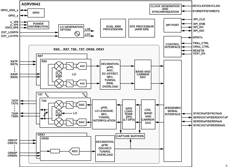
The ADRV9042 is a highly integrated, RF transceiver with an integrated, digital front end (DFE) designed for use in instrumentation and aerospace, defense applications, and advanced communications systems. The transceiver contains eight transmitters, two observation receivers, eight receivers, integrated LO and clock synthesizers, and digital signal processing functions. The ADRV9042 is a high performance and low power radio with DFE support that has been designed for use in general-purpose applications operating from low frequencies. The ADRV9042 has a tuning range from 600 MHz to 7125 MHz and covers all UHF, industrial, scientific, and medical (ISM) and cellular frequency bands including WiFi 6E. Support beyond these frequencies can be enabled via external upconverters and downconverters available at Analog Devices, Inc.
Please see the Data Sheet for the full description.
APPLICATIONS
- Tactical communications
- Phased array radars
- Electronic warfare
- Wireless test and measurement
- Portable instruments
- Time division duplexing (TDD)
- Frequency division duplexing (FDD)