购物车中还没有商品,赶紧选购吧!

 预发布
预发布
特性
- Integrated 1 Tx × 2 Rx RF transceiver
- Operating frequency range of 70 MHz to 6000 MHz
- Transmitter and wideband receiver signal bandwidth from 12 kHzto 40 MHz
- Narrowband receiver signal bandwidth from 12 kHz to 2 MHz
- 2 fully integrated, fractional-N, RF synthesizers
- 2 fully integrated, fractional-N, RF PLLs to control external VCO banks
- Supports external LO
- LVDS and CMOS synchronous serial data interface options
- Low power monitor and sleep modes
- Fully integrated DPD for narrowband waveforms
- User-programmable ARM core with 928 kB memory
- Interfaces include 2× UART, 2× I2S, I2C, QSPI, SPI, JTAG
- Library of hardware accelerators
- Fully programmable via a 4-wire SPI
- Package: 196-ball, 10 mm × 10 mm, CSP_BGA
产品详情和应用
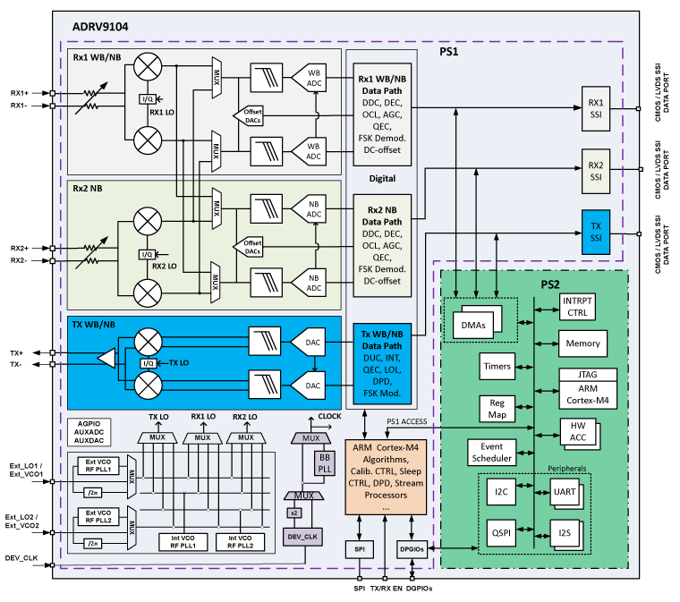
The ADRV9104 is a highly integrated RF transceiver with an integrated application processor that has a single transmitter, dual receivers, integrated synthesizers, and digital signal processing functions. Its a high performance, highly linear, high dynamic range transceiver designed for the lowest power consumption to support portable, and battery powered equipment. The ADRV9104 operates from 70 MHz to 6000 MHz and covers the VHF (from 70MHz),UHF, industrial, scientific, and medical (ISM) bands, and cellular frequency bands in narrow-band (kHz) and wideband operation up to 40 MHz. The ADRV9104 is capable of both TDD and uncalibrated FDD operation.
The transceiver has three direct conversion signal paths (1Tx and 2Rx) with state-of-the-art noise figure and linearity. The dedicated Narrow Band Receiver path can support up to 2MHz of RF signal BW. The dedicated wide band Receiver path can support up to 40MHz of RF signal BW. Each receiver and transmitter subsystem includes quadrature error correction (QEC), programmable digital filters, DC offset correction on the Rx paths and LO leakage suppression on the Tx path. In addition, functions such as analog-todigital converters (ADCs), digital-to-analog converters (DACs), and general-purpose inputs/outputs (GPIOs), are integrated to provide additional monitoring and control capability.
The transmitter has internal modulator functions that can support for typical Land Mobile Radio (LMR) standards, such as Analog FM, Digital Mobile Radio (DMR), P25. The modulator integrates the symbol mapping, interpolation and pulse shaping functions which allow the basedband processor to send 2bit symbols to ADRV9014.
The fully integrated phase-locked loops (PLLs) provide high performance, low power, fractional-N frequency synthesis for the transmitter, receiver, and clock sections. Careful design and layout techniques provide the isolation required in high performance p