购物车中还没有商品,赶紧选购吧!

 量产
量产
特性
- Saves Space (Optimized for High-Channel-Count Systems/Portable Systems)
- High Density
- 8 Channels (Five-Level Operation)
- Integrated Low-Power T/R Switches
- DirectDrive® Architecture Eliminates External High-Voltage Capacitor
- No External Floating Power Supply (FPS) Required
- High Performance (Designed to Enhance Image Quality)
- Excellent -40dBc (typ) THD for Second Harmonic at 5MHz
- High Bandwidth and Ultra-Fast Rise/Fall Edges Enable High-Order PWM Burst Shaping
- Sync Function Eliminates Effects of FPGA Jitter and Improves Performance in Doppler Mode
- Low Propagation Delay 11 (typ)
- Strong Active Return to Zero
- Saves Power
- Low Quiescent Power Dissipation (21mW/Channel in Octal Mode)
- Programmable Current Capability
- Shutdown Mode
产品详情和应用
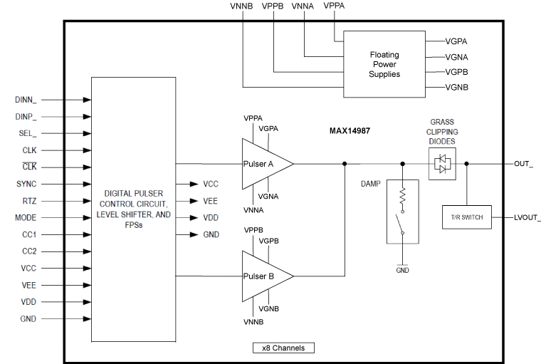
The MAX14987 octal five-level, high-volage (HV) pulser device generates high-frequency HV bipolar pulses (up to ±105V) from low-voltage control logic inputs for driving piezoelectric transducers in ultrasound systems. All eight channels have embedded overvoltage-protection diodes and an integrated active return-to-zero clamp. The device has embedded independent (floating) power supplies (FPS) and level shifters that allow signal transmission without the need for external HV capacitors. The device also features eight integrated transmit/receive (T/R) switches.
The device features two modes of operation: shutdown mode and octal five-level mode pulsing (with integrated active return-to-zero clamp). In octal five-level mode pulsing, each channel is controlled by three logic inputs (DINN_/DINP_/SEL_). Each channel features two HV half-bridges operating from independent pairs of voltage supplies (VPPA, VNNA and VPPB, VNNB) and sharing the same output. The half-bridge operating from VPPA, VNNA is named HB1 while the half-bridge operating from VPPB, VNNB is named HB2. The voltage rating is the same for the two half-bridges. They can both operate from 0 to ±105V.
HB1 is sized to provide a maximum driving current in excess of ±2.5A and is optimized in terms of Bandwidth and PWM performances.
HB2 is sized to provide a maximum driving current of ±1.6A and is normally intended to be used in Doppler modes (CWD, CFM, PWD). The driving current of HB2 can be programmed at 1.6A, 1.1A, 0.5A, and 0.3A. This allows reducing the power dissipation in particular for CWD modality. HB2 exhibits excellent jitter (< 6ps) and phase noise performances (156dBc @1kHz offset) in CWD modality.
The return-to-zero (clamp) driving current can also be programmed either at 1.25A or 2.5A by means of a dedicated CMOS input (RTZ).
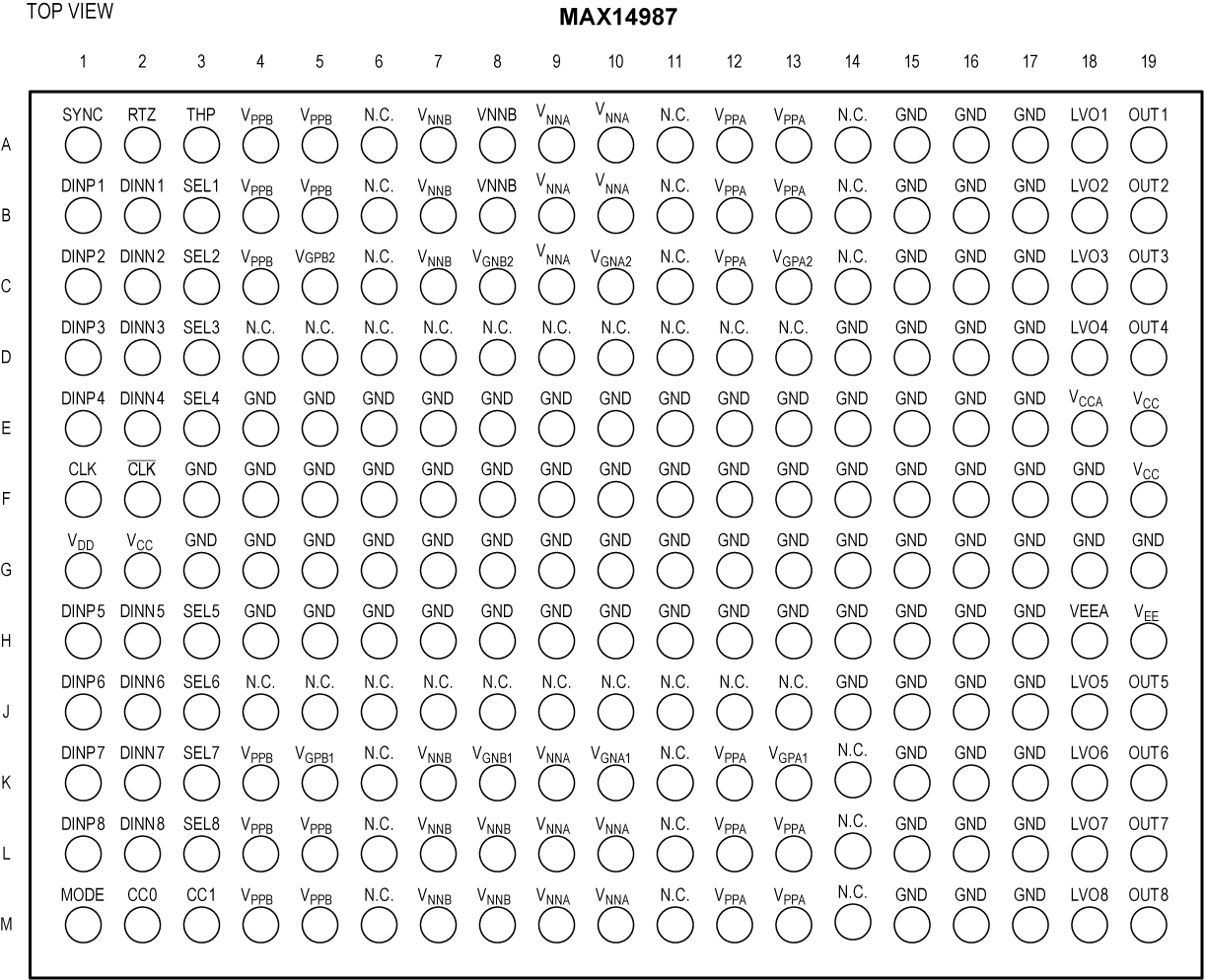
The device is available in a 228-bump (10mm x 16mm) BGA packag